A Comprehensive Overview of Ceramic PCB Manufacturing
A Comprehensive Overview of Ceramic PCB Manufacturing
15 Aug, 2022
By ren
Meta Description:
Do you know about the ceramic PCB manufacturing process? In this article, we have this content ready for you! Come and see!
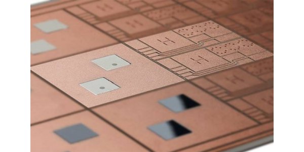
Ceramic PCB
The Properties of Ceramic PCB:
Traditional PCBs use fibreglass, epoxies, polystyrene, etc. as a substrate material that possesses polymeric properties. These PCBs use ceramic and possess the following properties:
Low coefficient of thermal Expansion
High thermal conductivity
Chemically stable
High erosion resistance
Good mechanical intensity
High tracing density
Manufacturing:
Ceramic PCBs are similar to other types of PCBs having stacked circuit layers with solder masks and silk screens. Ceramic PCBs manufacturing is difficult since the circuit layers cannot be produced on the surface of ceramic easily. Here are a few methods that we can use for ceramic printed circuit board manufacturing.
1. High temperature co-fired circuit:
This is one of the earliest manufacturing processes.
Material used:
Alumina, Aluminum nitride, mullite, etc.
Process:
Ceramic powder to be used in the manufacturing process is heated at 1300-1600° C to a point before its Liquification. It is then cooled or dried for solidification. If we need to make a hole in the ceramic surface, we can make it by drilling.
If we put metals such as tungsten, molybdenum and manganese at high temperatures, they will become melts. This high-temperature process is the basis for completing the material printing. And this allows for the design of a circuit layer. The amount of sintering additives such as titanium carbide and zirconia oxide is about 4-8%.
The whole product is then sintered at a high temperature of 1400-1600℃. It will form a ceramic circuit board. Finally, it needs a solder mask to protect its surface layer. Then use the silk screen to give it a better surface treatment.
High-temperature co-fired ceramics require high melting temperatures and hence circuit metal will have poor conductivity. Therefore, metals such as Cu, Ag and Au cannot be raw materials for the circuit layer of ceramic PCBs.
Therefore, HTCC is suitable for high-power circuits, but not for high-frequency circuits.
Pros:
This process provides adequate structural strength and chemical stability to the board.
It also offers high wiring density.
Cons:
It is an expensive process because of the high sintering temperature.
It also has poor circuit conductivity.
2. Direct Bonded Copper:
As the name shows that the metal used in this process is copper. The thickness of copper cladding is about 0.1 mm.
Material used:
Alumina, aluminium nitride, etc.
Process:
In nitrogen gas at temperatures from 1065 to 1083 C, the core of the copper cladding attaches directly to the base material.
Etching of the coating will replace the circuit layer of auxiliary sintering. Finally, it needs to add a solder mask to the surface.
In this process, some small bubbles may exist between the substrate and the circuit layer. This decreases the strength and some properties of the material. Also, it does not allow drilling. So, if you want holes in your design, you should use another method of manufacturing.
DBC technology is inexpensive and best in the case of batch production. It has a good thermal dissipation ability.
DBC reduces the size of the components and also enhances the power capacity of the circuit. Therefore, they require the packaging of electronic devices such as semiconductor refrigeration and LED.
Pros:
Cost-effective
High thermal conductivity
High adhesion strength
Easy to weld
Cons:
Poor accuracy
A hard and rough surface
Suitable for Batch production
Can’t make a drill
3. Thick Film PCB:
This processing results in the production of carbon resistors printed on the surface of the circuit board.
Material Used:
During this process, the material used is similar to DBC i.e. Alumina (98%), aluminium nitride, etc.
Process:
Firstly, draw a circuit diagram. Divide it into several parts and move them into the image of the circuit.
A template for thick film ceramic PCB is formed by using the photo imaging method.
When printing a design on a circuit board, it requires a thick layer of the template. This thick film paste is prepared from a mixture of organic adhesives, ceramic powders, silver, platinum, nickel, aluminium, and other metals and their alloys.
After the paste formation, it is printed on the base using the printing method.
It is then sintered at 1000 degrees Celsius. During this process, the organic binder starts decomposing and results in the formation of resistors. These resistors are clipped from the edges or sometimes according to the resistance required in the circuit. This is done by laser technology.
At last, adding a solder mask is a must for protection.
This technology is used where small size and less power are required. The minimum thickness of the film is 60 micrometres. So, a film having less thickness than 60 micrometres cannot be manufactured using this method.
Pros:
Smooth surface
Mechanical strength
High stability
high precision rate
Cons:
Poor electrical conductivity
3-D & fine circuits cannot be manufactured
4. Low-Temperature Co-fired Ceramic:
PCBs formed has multilayered and 3-D designs.
Material used:
Glass bonded ceramics, Glass-ceramic composite, etc.
Process:
For substrate, ceramic powder to be manufactured undergoes sintering at a very low operating temperature of about 900°C to form dense ceramic having precise thickness for thin film.
For holes, this compact raw material powder is drilled by laser.
Melted copper is poured into these holes and conductive paste is prepared to form a circuit layer using printing technology.
Since it uses a multi-layered structure, so lamination occurs.
After this, it undergoes sintering at 900° C to form a 3-D circuit.
Pros:
High conductivity
Little dielectric loss
Low temperature
Assembled easily
Cons:
Low thermal dissipation
Contraction problems
It is suitable for high-frequency communication devices.
5. Thin Film PCB:
The copper layer used in this process has a thickness of less than 1 mm.
Material used:
Al2O3, Al2N3, etc.
Process:
This process takes place in the presence of a vacuum. Moisture on the surface of ceramic is removed by providing heat.
A layer of copper metal is formed by using the magnetron sputtering technique. This technique also uses materials other than ceramic.
Photo resistance technology uses yellow light for the formation of circuit images on this layer. The remaining unwanted copper is removed by using an etchant.
This method is useful for packaging and for devices those that are small in size.
Pros:
Smooth surface
The low temperature required for manufacturing
Cons:
Cannot be used for 3-D structures
Expensive machinery
6. Direct Copper Plating:
This is done by using a thin film manufacturing process and the plating of copper increases its thickness.
It is used for solar cells, optical devices, semiconductors, etc.
Process:
Its manufacturing process is similar to thin film manufacturing with an unlimited thickness of the copper layer.
Pros:
Unlimited thickness
Fine circuit
Smooth surface finishing
Low operating temperature
Cons:
Expensive
Advantages of Ceramic PCB:
Ceramic PCB manufacturing is an easy and cost-effective method. Other than their conductivity and thermal expansion, they also have other advantages. These are:
Allows parallel processing
Can be operated at a high temperature
Excellent frequency behaviour
Dense packaging that protects against moisture
Applications:
Transmission:
Receiving or transmitting modules are produced by ceramic PCB for radar. The material mainly used in this process is Aluminum nitride which offers good thermal conductivity and low thermal expansion.
Memory components:
Missiles, aerospace, and telecommunication devices use ceramic PCBs memory modules. This provides high density and reliability along with shock resistance thus resulting in increased properties.
It is widely used in both analog and digital circuits.
Why You Need a Good Single-Layer PCB Service Provider:
Ifyou want your products to be of high quality make sure you connect to a good service provider. All the design and manufacturing process is although bit easy but it requires experts and professionals to make sure that the final product is either capable enough to be launched in the market. Does it meet all the standards? If you want professional behaviour and good service, then here is good news for youbecause Europe PCB is known to provide the best services and they are known as one of the great service providers of PCB assembly manufacturers all around Europe and provide their services in SMT & DIP and much more.
Europe PCB provides fast and in-time delivery services with effective cost.
There is a team of professionals and experts in the engineering and supply chain fields in Europe PCB.
They have the best inspection equipment to ensure the quality of the product.
They have the departments of quality assurance and quality control to endure the best services.
To make sure the satisfaction of customers is met, Europe PCB provides its customer with a quick response so their queries can be dealt with efficiently.
Europe PCB will provide you with highly satisfying products with good customer service as well. You can choose according to the product requirement which manufacturing method is to be used.