

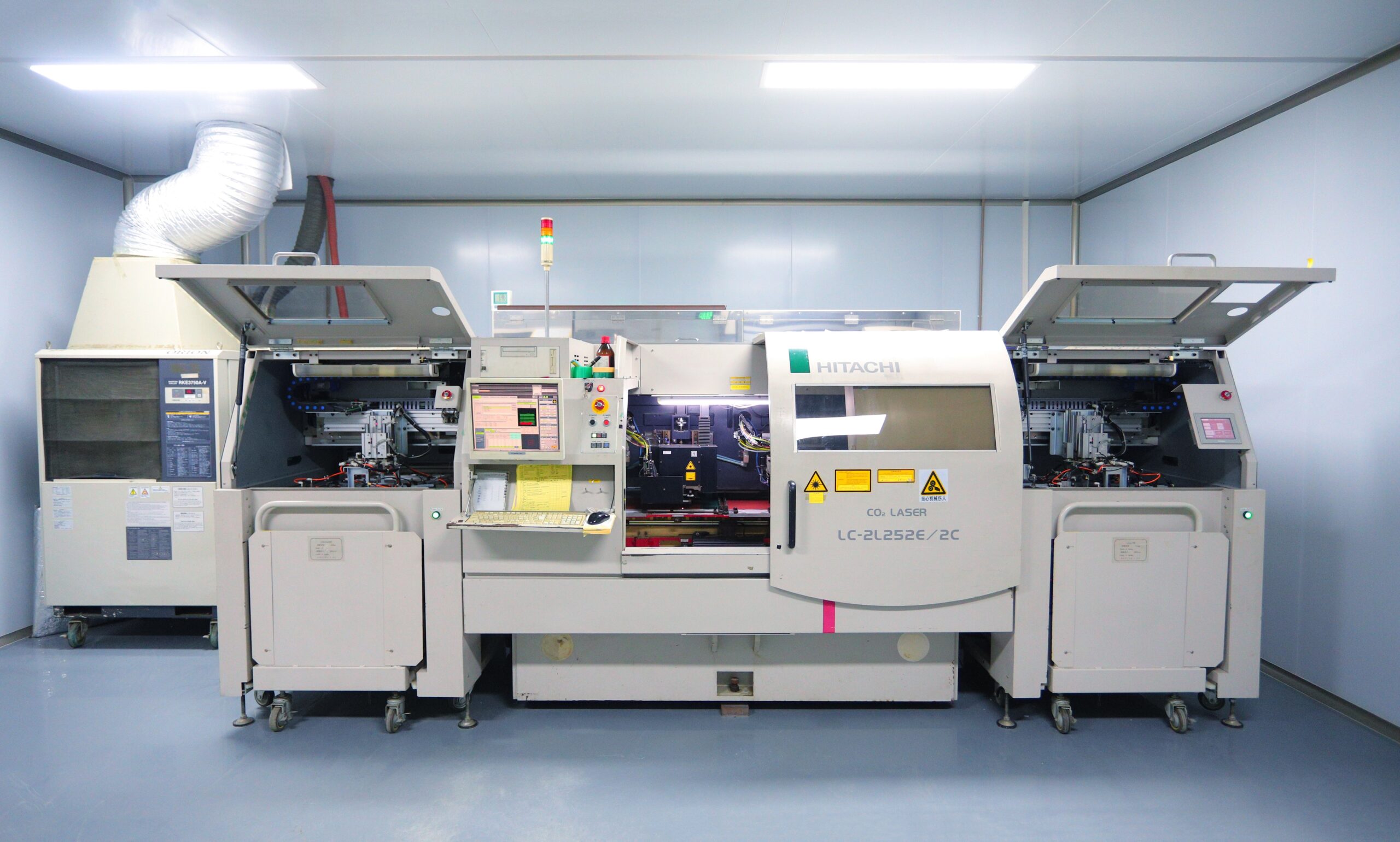
Hitachi's laser drill crushes HDI production! It nails micro via precision, zipping through copper/resin with tight tolerances. Handles diverse hole sizes, maintains consistency across high-density layouts. Fast, reliable, and built to ace the intricate demands of HDI PCB manufacturing.
We have two VCP production lines, one for through-hole copper plating and the other for laser hole filling of HDI products. We use the most advanced equipment in China, ensuring uniform copper plating with good uniformity, which provides a stable foundation for subsequent production.
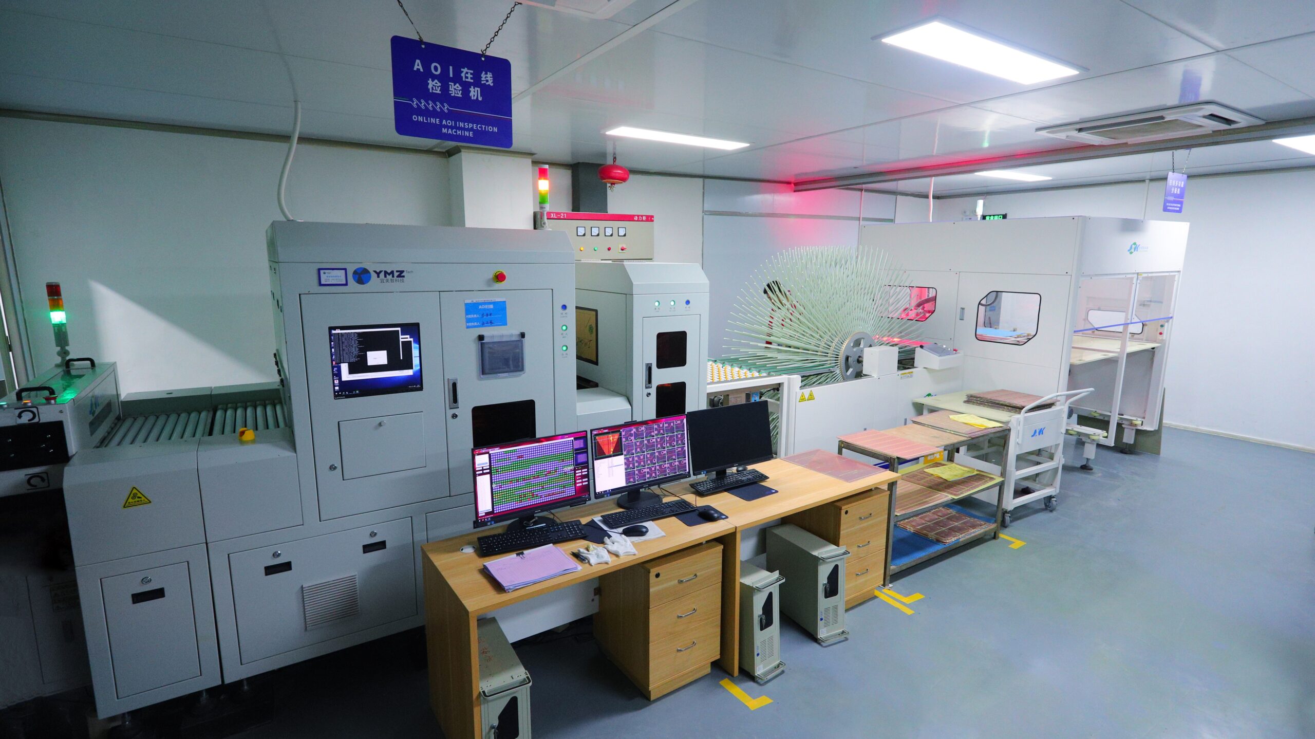
Our online AOI for PCB etching can inspect line defects with extremely high precision. Its automatic sorting arm can pick quickly, greatly reducing manual work. The output has been increased, errors have been reduced, and the yield rate of finished products has been greatly improved.
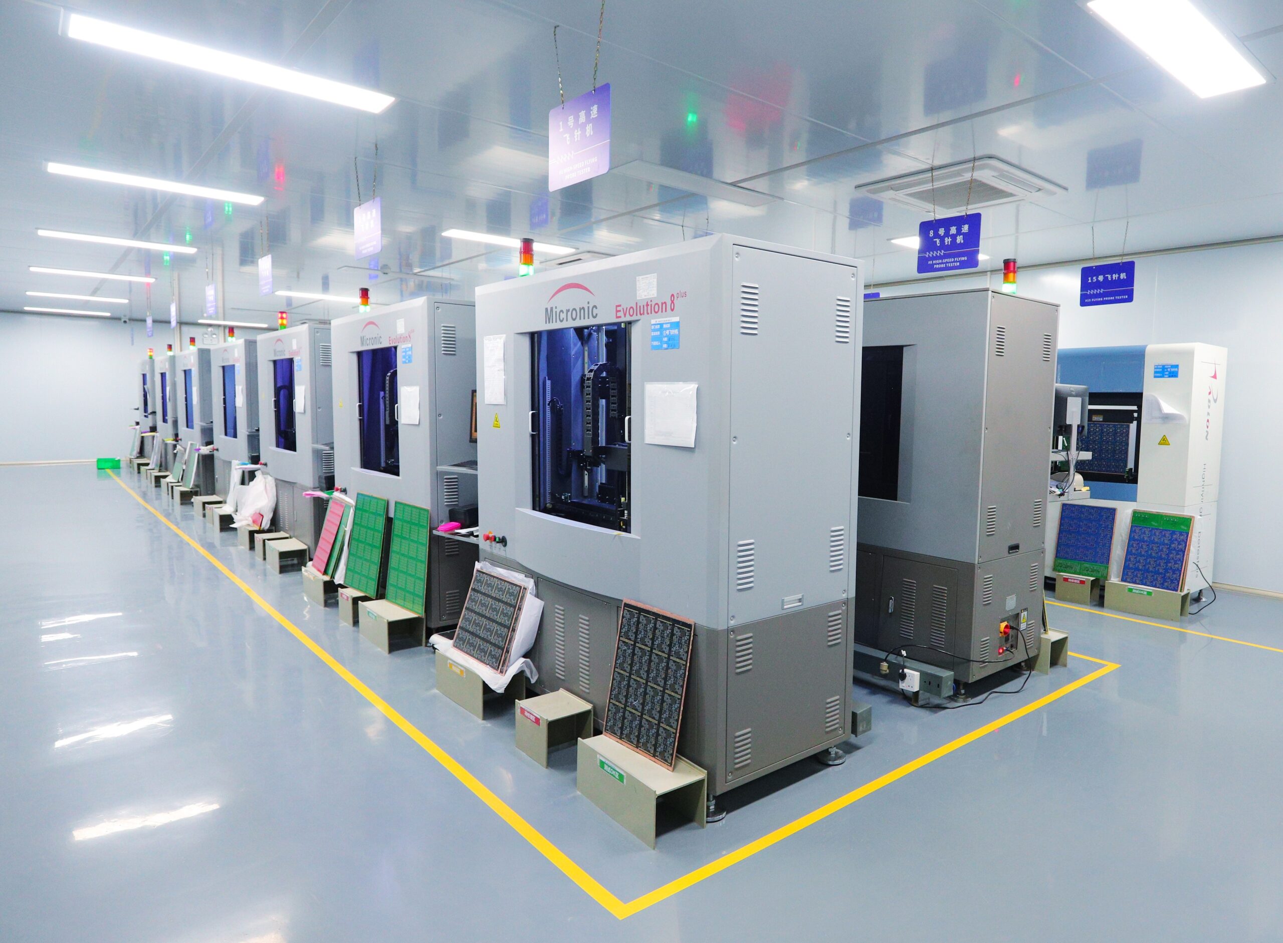
Our flying probe test department runs on all-screw machines—total workhorses. High precision, blazing speed, including 8-probe setups. They crank up efficiency for fast turnaround, nailing quality checks while slashing lead times. Perfect for keeping your PCB deliveries on point.
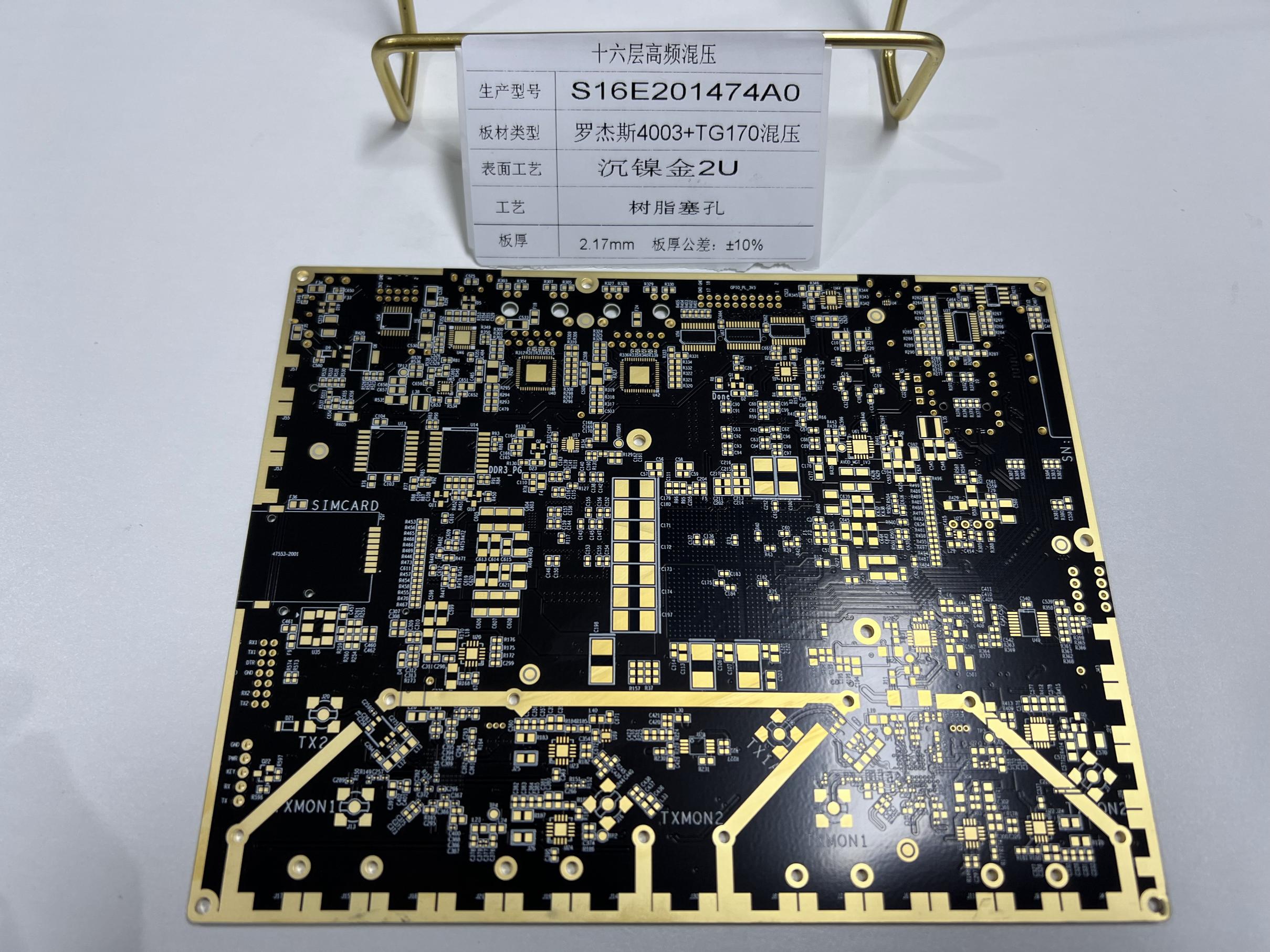
We have multiple linear motor drilling machines with a minimum drilling hole diameter of 0.1MM, including high-performance depth control drilling machines for back drilling, which are fast and highly precise, suitable for high-difficulty products such as HDI and rigid-flex PCBS.
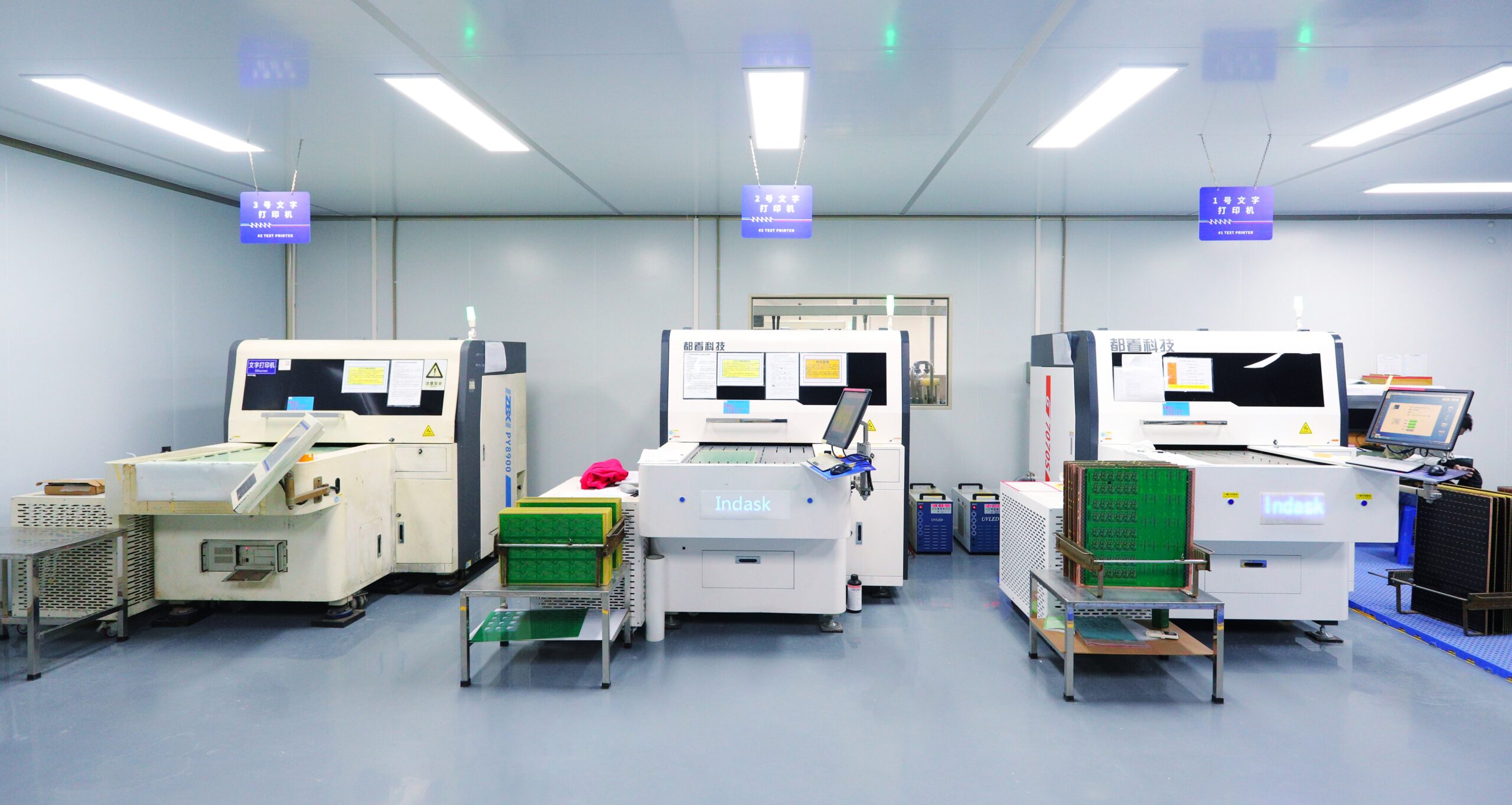
Silkscreen Printer has higher precision, with a resolution of up to 0.05mm. The character edges are clear, which can meet the fine marking requirements of high-density PCBS. It is more efficient for small-batch and multi-variety order switching and shortens the production change time.
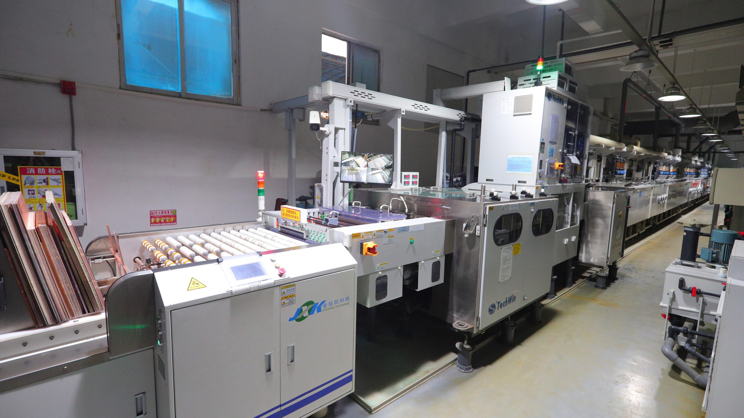
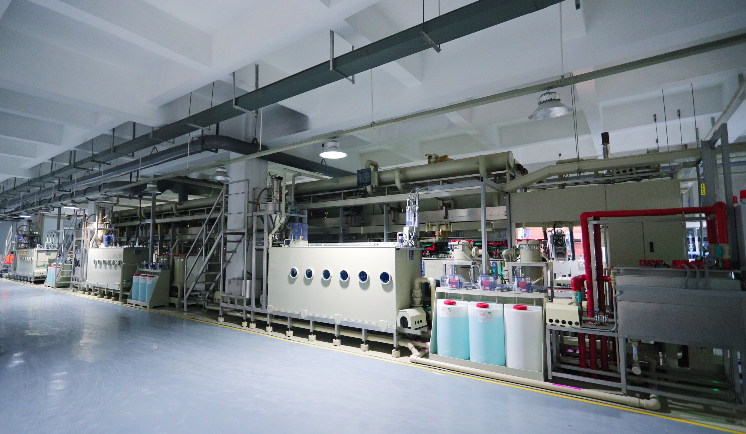
For Immersion copper , we adopt a Horizontal Electroless Copper Plating line. Its advantages include good uniformity, high continuous production efficiency, strong adaptability suitable for different materials and high-precision products such as HDI, and a high degree of automation, reducing reliance on personnel.
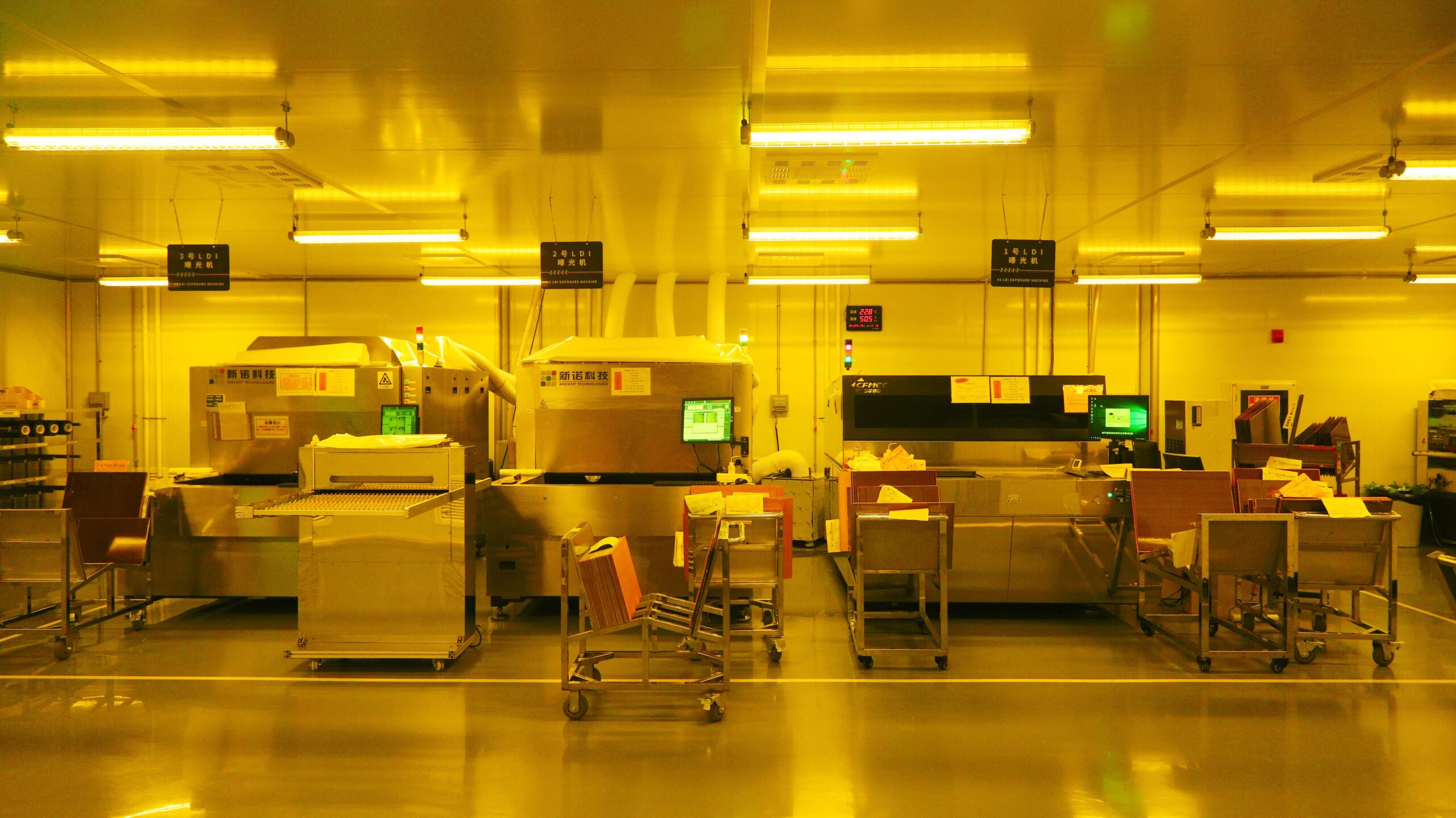
"Both our circuit and solder mask production lines use LDI exposure machines, cutting down on film usage and management. With laser imaging resolution down to 0.05mm, they boost efficiency and reduce waste."
Professional chemical laboratories strictly control the quality of chemical reagents or the production line.Through scientific methods such as spectral analysis and component titration, they ensure that every drop of reagent meets the process standards,guaranteeing product quality from the source.
By using multiple methods such as flying probe testing, test fixture testing, four-wire testing, and appearance testing, the electrical performance,soldering quality, and circuit integrity of HDl circuit boards are comprehensively inspected to ensure that the products are 100% qualified before leaving the factory.
Equipped with high-precision flying probe testers,intelligent AOl optical inspection instruments, optical microscopes, impedance testers, hole copper testers, AVl and other professional equipment, from raW material entry to finished product exit,360 all-round inspection is carried out, leaving no minor defects overlooked.